Chinese semiconductor firm expands with $1. 15 billion chip packaging plant
Amid rising domestic demand for semiconductors fueled by the rapid expansion of AI, China’s JCET has announced plans to invest $1. 15 billion in a new manufacturing facility in Shanghai. The Chinese. . .
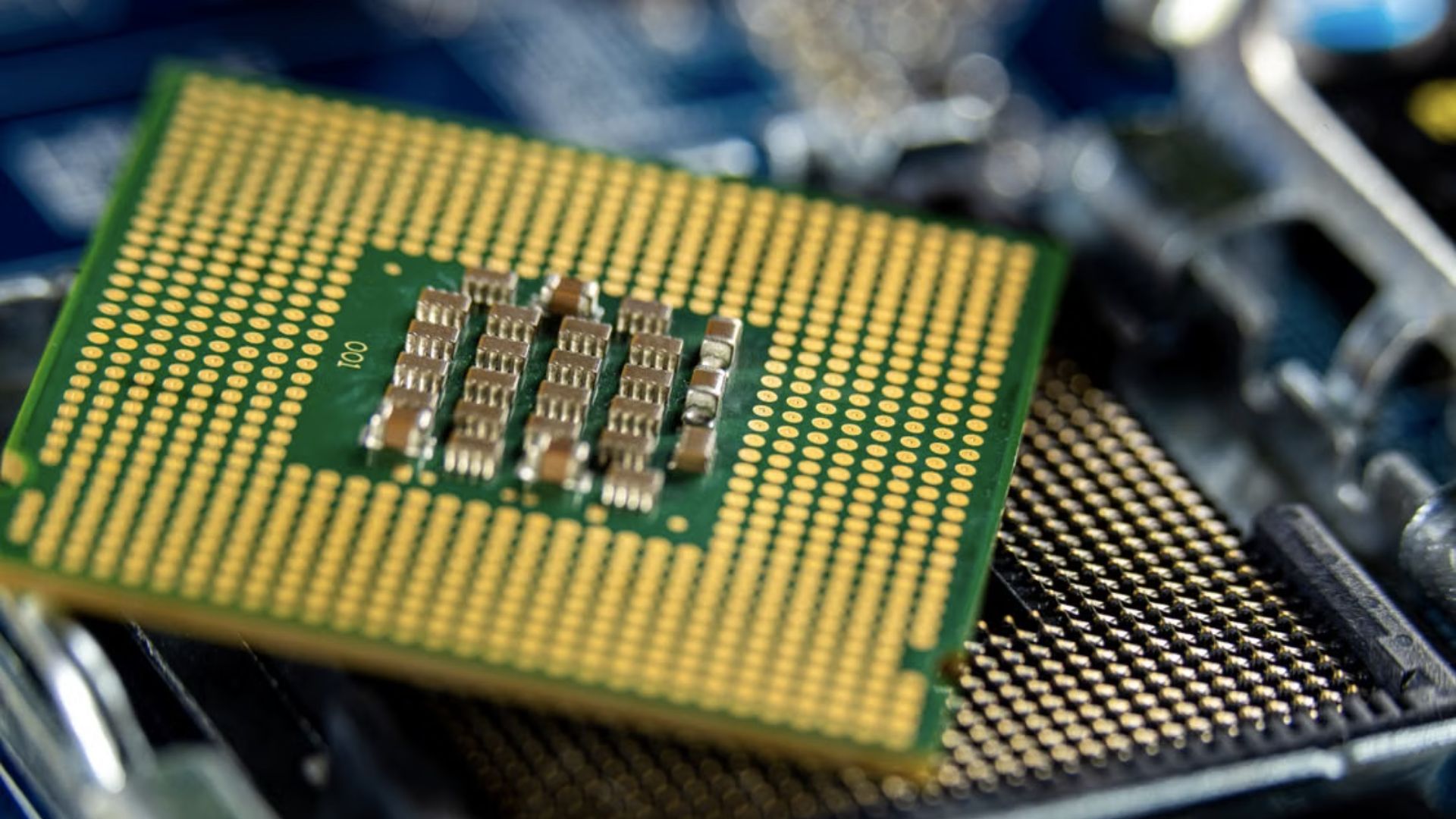
Amid rising domestic demand for semiconductors fueled by the rapid expansion of AI, China’s JCET has announced plans to invest $1. 15 billion in a new manufacturing facility in Shanghai. The Chinese chip-packaging and testing giant said the project will be developed through a controlled subsidiary with registered capital of roughly $560 million. Located in Shanghai’s Lingang Special Area, the new plant will focus on advanced chip packaging and testing technologies aimed at strengthening China’ssemiconductorsupply chain. The project will be completed in two phases, with the first phase covering factory construction and equipment installation, scheduled for completion in the second half of 2028. China’s chip push gains momentumJCET said the new investment is designed to accelerate the expansion of its high-end advanced packaging capabilities while strengthening its broader market position. Headquartered in China’s eastern Jiangsu province, the company sees advanced packaging as a strategic priority as demand grows for more powerful and efficient chips,the South China Morning Postreported. The process, which represents the final stage of semiconductor manufacturing by integrating individual chip dies into finished products, has become increasingly important to China’s efforts to strengthen domesticchipproduction and reduce dependence on foreign technology. Beijing’s push to strengthen its domestic semiconductor industry has become more urgent as US export restrictions continue to limit access to leading chip manufacturing facilities such as Taiwan Semiconductor Manufacturing Company (TSMC). Against this backdrop, investor confidence in JCET has surged, with the company’s shares listed in Shanghai climbing 147 percent since the start of the year, driven by strong business growth and rising demand foradvancedchip technologies. Advanced packaging to drive the next era of chip innovationSpeaking at the Semicon China conference in March, JCET’s CEO Zheng Li emphasized that advanced packaging is emerging as one of the most important drivers of semiconductor innovation. He noted that the industry is increasingly operating in a post-Moore’s Law era, where simply reducing transistor sizes no longer delivers the same steady improvements in computing performance. As traditional scaling becomes more difficult and expensive, advancedpackagingis gaining importance by enabling chipmakers to combine multiple chiplets and architectures into more powerful, energy-efficient systems, opening new paths for performance gains in AI and high-performance computing. According to Zheng, the semiconductor industry is undergoing a fundamental shift, with the focus moving away from simply increasing transistor density toward improving overall chip quality and performance. He explained that next-generation packaging technologies are expected to play a critical role in this transition, particularly by enabling far greater precision in chip integration. He also noted that emerging packaging methods aim to reduce surface roughness to below 0. 2 nanometers, a significant improvement over the roughly 5 nanometers associated with current 2. 5D packaging technology.